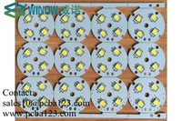
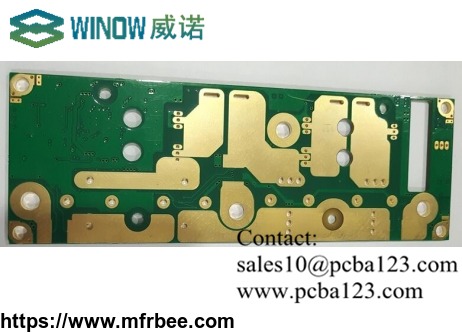
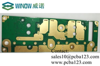
5 Oz Heavy Copper Printed Circuit Board
Product Quick Detail
- Minimum Order
- 1
- Place Of Origin
- China (Mainland)
- Packaging
- N/A
- Delivery
- N/A
Specifications
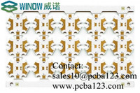
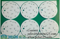
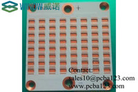
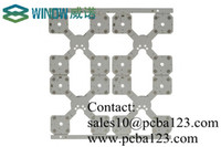
Heavy Copper PCB
Heavy copper PCB products are used extensively in power electronic devices and power supply systems. A growing trend in the PCB industry, this unique type of thick copper PCB features a finished copper weight of more than 3oz (105μm), compared to the 1oz (35μm) or 2oz (70μm) copper weight generally found in those with a standard PCB copper thickness.
The additional copper PCB thickness enables the board to conduct a higher current, achieve good thermal distribution and implement complex switches in a limited space. Other advantages include increased mechanical strength at connector sites, the ability to create a smaller product size by incorporating multiple weights on the same layer of circuitry and the ability to use exotic materials to their maximum capacity with minimal risk of circuit failure.
- Country: China (Mainland)
- Market: Americas,Europe,Asia,European Union
- Founded Year: 1999
- Contact: Lucina Lu