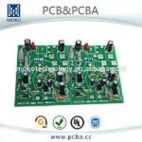
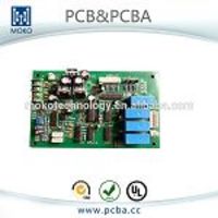
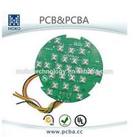
Reliable 8 Layer GPS Receiver Printed Circuit Board


Product sourcing details
Supplier: Moko Technology Ltd
Purchasing information
- Minimum order
- 1
- Lead time
- 15 Days
Please confirm with the supplier: Model / reference, Key specifications / compatibility, Samples, Export markets, Supply capacity.
Specifications
Place of Origin: Guangdong, China (Mainland)
Brand Name: GPS PCB
Model Number: EW-50906S02
Number of Layers: 8-Layer
Base Material: FR4
Copper Thickness: 0.5-5 OZ
Board Thickness: 0.4 to 6.0mm(4 to 240mil)
Min. Hole Size: 0.025mm
Min. Line Width: 0.075mm(3mil)
Min. Line Spacing: 0.075mm(3mil)
Surface Finishing: HASL, ENIG
Max Panel size: 800*508mm
Board finished thickness: 0.2-4.0mm
Tolerance of finished panel thickness: ±10%
Surface Treating Process of Inner layer: Brown Oxide
Layer Count: 1-18
Impedance control and tolerance: 50Ω±10%
Peel strength of line: ≥107g/mm
Wrap and twist: ≤0.5%
Standard: IPC-A-610D
Service type: One-stop turnkey service .
http://www.protelpcb.com
- Company: Moko Technology Ltd
- Country: China (Mainland)
- Address: 4F,Building2,Guanghui Technology Park,MinQing Rd,Longhua,Shenzhen,China
- Contact: jennyzhang jennyzhang