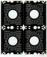
Multilayer PCB Up to 64 Layers; FR4 TG135/TG150/TG170; Halogen Free/CTI≥600; Aspect Ratio (Finish Hole) 28:1; Sample Expedited 8 Hours(1-2Layer); HDI PCB Blind/Buried/Hybrid Via; 5+N(N+M)+5 Structure; Trace Width/Spacing 1.6/1.6mil; Laser Hole Size(mm)≥0.075; High Density ...
Number of layers: 8 Surface finish: ENIG Base material: FR4 Outer Layer W/S: 4/3mil Inner layer W/S: 4/3mil Thickness: 1.2mm Min. hole diameter: 0.2mm Special process: impedance control Advantages Of 8 Layer PCB Own lamination process to convenient production for Multilayer PCB ...
HDI PCB Blind/Buried Via 5+N(N+M)+5 Structure Trace Width/Spacing 1.6/1.6mil Laser Hole Size(mm)≥0.075 High Density Interconnector Founded in 2007,PEAK ...
Previous image Next image Number of layers: 16 Surface finish: ENIG Base material: FR4 Thickness: 3.0mm Min. hole diameter:0.35mm size:420×560mm Outer Layer W/S: 4/3mil Inner layer W/S: 5/4mil Aspect Ratio: 9:1 Special process: via-in-pad Impedance Control Press Fit Hole ...
Previous image Next image Number of layers: 10 Surface finish: ENIG Aspect Ratio: 8:1 Base material: FR4 Outer Layer W/S: 4/4mil Inner layer W/S: 5/3.5mil Thickness: 2.0mm Min. hole diameter:0.25mm Special process: Impedance Control, Resin Plugging, Different Copper Thickness ...
Number of layers: 8 Surface finish: ENIG Base material: FR4 Outer Layer W/S: 4/3mil Inner layer W/S: 5/4mil Thickness: 1.6mm Min. hole diameter: 0.2mm Special process: half hole Advantages Of 8 Layer ENIG Half Hole Custom Made PCB Own lamination process to convenient production ...
Number of layers: 4 Surface finish: ENIG Base material: FR4 Outer Layer W/S: 6/4mil Inner layer W: 21mil Thickness: 0.4mm Min. hole diameter: 0.2mm Special process: impedance control+half hole Advantages Of 4 Layer ENIG Impedance Control Half Hole PCB Electric Circuit Board Own ...
Number of layers: 4 Surface finish: ENIG Base material: FR4 Outer Layer W/S: 6/3.5mil Inner layer W/S: 6/4mil Thickness: 0.8mm Min. hole diameter: 0.28mm Special process: impedance control+half hole Advantages Of 4 Layer ENIG Impedance Control Half Hole Fr4 PCB Own lamination ...
Number of layers: 2 Surface finish: OSP Base material: FR4 Outer Layer W/S: 6/4mil Thickness: 1.0mm Min. hole diameter: 0.25mm Special process: impedance control+half hole Advantages Of 2 Layer OSP Impedance Control Half Hole PCB Own lamination process to convenient production ...
Number of layers: 2 Surface finish: ENIG Base material: FR4 Outer Layer W/S: 7/4mil Thickness: 1.0mm Min. hole diameter: 0.3mm Special process: impedance control+half hole Advantages Of 2 Layer ENIG Impedance Control Half Hole PCB Product Own lamination process to convenient ...