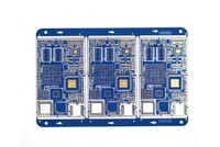
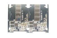
Via In Pad Fr4 PCB

FOB Price
USD $30.00 / Piece
Place Of Origin
china
Minimum Order
1
Packaging
N/A
Delivery
15 Days
Via In pcb board material fr4, using copper plating or epoxy to fill holesfor circuit board factor, prevent solder paste or flux from flowing into the via in pad, avoid solder ball getting into via or solder mask cover on pad and cause false soldering. HUIHE CIRCUITS Via In Pad Fr4 PCB has passed ISO9001/ISO13485/IATF16949/UL/RoHS/REACH certification.
What Is A Hole-In-The-Panel Circuit Board?
The hole in the disk is an important part of the multi-layer PCB. It is not only responsible for the main functions of the PCB, but also the cost of drilling usually accounts for 30% to 40% of the PCB manufacturing cost. In short, the holes pressed on the pads on the PCB can all be called holes in the disk.
Processing Requirements For Hole Plugs In The Disk
No solder mask ink entering the hole
There should be no tin beads hidden in the hole
No explosive oil, ink pads, making it difficult to mount components, etc.
Common Sense Of Circuit Board Plug Hole
Prevent the tin from penetrating the component surface from the via hole to cause a short circuit when the PCB is wave soldered
Avoid flux residue in the vias
Prevent the tin balls from popping up during wave soldering, causing short circuits
Prevent surface solder paste from flowing into the hole, causing false soldering and affecting placement

Huihe Circuits is a professional pcb circuit manufacturer, we provide fr4 circuit board material, fr4 circuit board manufacturing, fr4 pcb board, fr4 pcb datasheet, fr4 pcb sheet, fr4 pcb thickness, pcb manufacturing service and etc. For more information, please feel free to contact us!

  • Country: China (Mainland)
  • Business Type: Manufacturer
  • Market:
  • Founded Year:2017
  • Address:Building 2, Xinda Park, Lvyuan Road, Xinfeng County, Ganzhou 341600, Jiangxi
  • Contact:Huihe Circuits
more images of Via In Pad Fr4 PCB
*Your name:
*Your Email:
*To:Xinfeng Huihe Circuits Co., Ltd.
*Subject:
*Message:
Enter between 20 to 3,000 characters. English only.     Characters : 0 / 3000
*Enter the secure code shown below Mfrbee security Image      Reload Image

submiting now We do inquire for you , please wait ...

FR4 PCB
FR4 PCB

What is FR4? FR4 is the name of a type of epoxy glazing material. fr stands for flame retardant. 4 refers to the factors that differentiate it from other materials. FR4 means two things. The material. As a construction material, it refers to epoxy laminates reinforced with ...

GreensTone (Shenzhen) Electronics Co., Limited

fr4 pcb
fr4 pcb

What is FR4? FR4 is the name of a type of epoxy glazing material. fr stands for flame retardant. 4 refers to the factors that differentiate it from other materials. FR4 means two things. The material. As a construction material, it refers to epoxy laminates reinforced with ...

GreensTone (Shenzhen) Electronics Co., Limited

4 Layer ENIG Impedance Control Half Hole Fr4 PCB

Number of layers: 4 Surface finish: ENIG Base material: FR4 Outer Layer W/S: 6/3.5mil Inner layer W/S: 6/4mil Thickness: 0.8mm Min. hole diameter: 0.28mm Special process: impedance control+half hole Advantages Of 4 Layer ENIG Impedance Control Half Hole Fr4 PCB Own lamination ...

Xinfeng Huihe Circuits Co., Ltd.

4 Layer FR4+Rogers ENIG PCB

Number of layers: 4 size:80*88mm Surface finish: ENIG Base material: Rogers FR4 4350B Min. hole diameter: 0.3mm Minimum Line Width:0.230mm Minimum Line Space:0.170mm Thickness: 1.0mm Advantages Of 4 Layer Rogers FR4 PCB Own lamination process to convenient production for ...

Xinfeng Huihe Circuits Co., Ltd.

6 Layer HASL Blind Buried Via PCB

Number of layers: 6 Surface finish: HASL Base material: FR4 Outer Layer W/S: 9/4mil Inner layer W/S: 11/7mil Thickness:1.6mm Min. hole diameter: 0.3mm Special process: Blind Vias Advantages Of 6 Layer HASL Blind Buried Via PCB Own lamination process to convenient production for ...

Xinfeng Huihe Circuits Co., Ltd.

14 Layer Blind Buried Via PCB

Number of layers: 14 Surface finish: ENIG Base material: FR4 Outer Layer W/S: 4/5mil Inner layer W/S: 4/3.5mil Thickness: 1.6mm Min. hole diameter: 0.2mm Special process: Blind & Buried Vias Advantages Of 14 Layer PCB Own lamination process to convenient production for ...

Xinfeng Huihe Circuits Co., Ltd.

10 Layer ENIG Blind Vias PCB

Number of layers: 10 Surface finish: ENIG Base material: FR4 W/S: 4/4mil Thickness: 1.6mm Min. hole diameter: 0.2mm Special process: Blind Vias Advantages Of 10 Layer ENIG Blind Vias PCB Own lamination process to convenient production for Multilayer PCB and shorten the lead ...

Xinfeng Huihe Circuits Co., Ltd.

Blind Buried Vias & Hdi Pcb

Buried vias PCB & blind vias PCB, use micro blind vias to increase the trace distribution density. Improve radio frequency, electromagnetic wave interference and hear conduction. Apply to computer server, mobile phone and digital camera products.HUIHE CIRCUITS is China HDI PCB ...

Xinfeng Huihe Circuits Co., Ltd.

4 Layer FR4+Rogers ENIG PCB

Number of layers: rogers fr4 size:80*88mm Surface finish: ENIG Base material: FR4+Rogers 4350B Min. hole diameter: 0.3mm Minimum Line Width:0.230mm Minimum Line Space:0.170mm Thickness: 1.0mm Advantages Of 4 Layer rogers fr4 pcb Own lamination process to convenient ...

Xinfeng Huihe Circuits Co., Ltd.