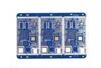
2 Layer F4B ENIG PCB


Product Quick Detail
- FOB Price
- USD $10.00 / Piece
- Minimum Order
- 1
- Place Of Origin
- china
- Packaging
- N/A
- Delivery
- 15 Days
Specifications
Number of layers: 2
Surface finish: ENIG
Base material: F4B
Min. hole diameter: 0.8mm
Outer Layer W: 6mil
Outer layer S: 6mil
Thickness: 1.0mm
Advantages Of 2 Layer F4B PCB
Own lamination process to convenient production for Multilayer PCB and shorten the lead time.
Jiangxi facility is environmental-friendly approved by the government .
Famous raw materials brand, Kingboard, Shengyi, ITEQ, Taiyo, Guangxin.
Highly automated production line with AIO Optical Scanning, Electroplating Automatic Line, High-speed flying probe test machines and inkjet printer.
Engineers with more than 15 years of experience
Customers located in more than 20 countries, the common choice of 500 high-end companies.
High staff stability, low mobility.
UL/ISO9001/SGS/IATF16949/ROHS/ISO1400 certificated.
Sales office in Shenzhen and own 12,000sqm factory in Jiangxi.
Establish an e-commerce system to reduce transaction costs and increase market response speed.
Packing And Delivery Of 6 Layer ENIG Impedance Control PCB.
There are many custom circuit board manufacturers, but we are one of the best choices for you.
- Country: China (Mainland)
- Business Type: Manufacturer
- Founded Year: 2017
- Address: Building 2, Xinda Park, Lvyuan Road, Xinfeng County, Ganzhou 341600, Jiangxi
- Contact: Huihe Circuits