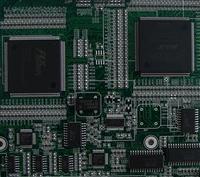
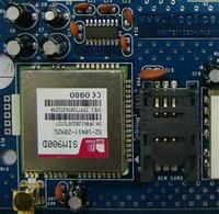
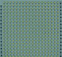
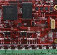
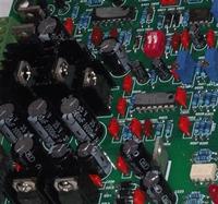
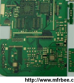
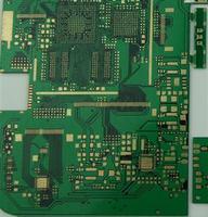
6 Layers PCB

Packaging
12
Delivery
15 Days
6 layers PCB ROHS PCB http://www.polariscircuit.com/
  • Country: China (Mainland)
  • Business Type:
  • Market:
  • Founded Year:1995
  • Address:Zhonghuacheng Building, Weiming South Street, Qiaoxi District
  • Contact:Jian Zhu
more images of 6 Layers PCB
*Your name:
*Your Email:
*To:Polaris Technology Co.,Ltd
*Subject:
*Message:
Enter between 20 to 3,000 characters. English only.     Characters : 0 / 3000
*Enter the secure code shown below Mfrbee security Image      Reload Image

submiting now We do inquire for you , please wait ...

1.8mm Thickness Immersion Gold 1u Regular 6 Layers PCB

Multilayer PCB Up to 64 Layers; FR4 TG135/TG150/TG170; Halogen Free/CTI≥600; Aspect Ratio (Finish Hole) 28:1; Sample Expedited 8 Hours(1-2Layer); HDI PCB Blind/Buried/Hybrid Via; 5+N(N+M)+5 Structure; Trace Width/Spacing 1.6/1.6mil; Laser Hole Size(mm)≥0.075; High Density ...

Shenzhen PEAK Technology Co., Ltd

8 Layer ENIG Impedance Control PCB

Number of layers: 8 Surface finish: ENIG Base material: FR4 Outer Layer W/S: 4/3mil Inner layer W/S: 4/3mil Thickness: 1.2mm Min. hole diameter: 0.2mm Special process: impedance control Advantages Of 8 Layer PCB Own lamination process to convenient production for Multilayer PCB ...

Xinfeng Huihe Circuits Co., Ltd.

High Quality Over 10 Layer High Tech HDI PCB Circuit Board Manufacturer

HDI PCB Blind/Buried Via 5+N(N+M)+5 Structure Trace Width/Spacing 1.6/1.6mil Laser Hole Size(mm)≥0.075 High Density Interconnector Founded in 2007,PEAK ...

Shenzhen PEAK Technology Co., Ltd

16 Layer ENIG Press Fit Hole PCB

Previous image Next image Number of layers: 16 Surface finish: ENIG Base material: FR4 Thickness: 3.0mm Min. hole diameter:0.35mm size:420×560mm Outer Layer W/S: 4/3mil Inner layer W/S: 5/4mil Aspect Ratio: 9:1 Special process: via-in-pad Impedance Control Press Fit Hole ...

Xinfeng Huihe Circuits Co., Ltd.

10 Layer Impedance Control Resin Plugging PCB

Previous image Next image Number of layers: 10 Surface finish: ENIG Aspect Ratio: 8:1 Base material: FR4 Outer Layer W/S: 4/4mil Inner layer W/S: 5/3.5mil Thickness: 2.0mm Min. hole diameter:0.25mm Special process: Impedance Control, Resin Plugging, Different Copper Thickness ...

Xinfeng Huihe Circuits Co., Ltd.

8 Layer ENIG Half Hole Custom PCB

Number of layers: 8 Surface finish: ENIG Base material: FR4 Outer Layer W/S: 4/3mil Inner layer W/S: 5/4mil Thickness: 1.6mm Min. hole diameter: 0.2mm Special process: half hole Advantages Of 8 Layer ENIG Half Hole Custom Made PCB Own lamination process to convenient production ...

Xinfeng Huihe Circuits Co., Ltd.

4 Layer ENIG Impedance Control Half Hole PCB Electric Circuit Board

Number of layers: 4 Surface finish: ENIG Base material: FR4 Outer Layer W/S: 6/4mil Inner layer W: 21mil Thickness: 0.4mm Min. hole diameter: 0.2mm Special process: impedance control+half hole Advantages Of 4 Layer ENIG Impedance Control Half Hole PCB Electric Circuit Board Own ...

Xinfeng Huihe Circuits Co., Ltd.

4 Layer ENIG Impedance Control Half Hole Fr4 PCB

Number of layers: 4 Surface finish: ENIG Base material: FR4 Outer Layer W/S: 6/3.5mil Inner layer W/S: 6/4mil Thickness: 0.8mm Min. hole diameter: 0.28mm Special process: impedance control+half hole Advantages Of 4 Layer ENIG Impedance Control Half Hole Fr4 PCB Own lamination ...

Xinfeng Huihe Circuits Co., Ltd.

2 Layer OSP Impedance Control Half Hole PCB

Number of layers: 2 Surface finish: OSP Base material: FR4 Outer Layer W/S: 6/4mil Thickness: 1.0mm Min. hole diameter: 0.25mm Special process: impedance control+half hole Advantages Of 2 Layer OSP Impedance Control Half Hole PCB Own lamination process to convenient production ...

Xinfeng Huihe Circuits Co., Ltd.

2 Layer ENIG Impedance Control Half Hole PCB

Number of layers: 2 Surface finish: ENIG Base material: FR4 Outer Layer W/S: 7/4mil Thickness: 1.0mm Min. hole diameter: 0.3mm Special process: impedance control+half hole Advantages Of 2 Layer ENIG Impedance Control Half Hole PCB Product Own lamination process to convenient ...

Xinfeng Huihe Circuits Co., Ltd.