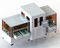
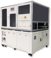
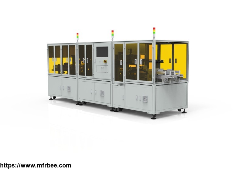
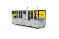
AOI DCB Automatic Ceramic Substrate Defect Inspection Equipment
Product Quick Detail
- Sample Thickness
- 1-2mm
- Object Size
- Max:190×140mm
- Weight
- 1500kg
- Detectable Flaw
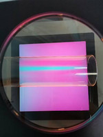
- short-circuit,connecting line, chipped edge, residual copper,
- Inspecting Speed
- 9.6s/pcs
- Suitable Object
- DCB
- Dimension
- 1930mm (L) ×1430mm (W) × 1900mm (H)
- Packaging
- 1 pcs in 1 carton
- Delivery
- 90 days
Specifications
| NO | Item | Parameter |
| 01 | Suitable object | DCB |
| 02 | Object size | Max:190×140mm; |
| 03 | Sample thickness | 1-2mm |
| 04 | CCDPixel | AOI 1:13um/Pixel AOI 2/3:24um/Pixel |
| 05 | Board warpsolution | Auto focus |
| 06 | CAM format | Gerber |
| 07 | Image Processingmethod | CCDColor software |
| 08 | InspectingSpeed | 9.6s/pcs |
| 09 | Data source | CAM+graphic scanning |
| 10 | Auxiliary function | Laser marking |
| 11 | Defect Confirmation | AOIon-line |
| 12 | Positioning Way ofceramic substrate | Automatic |
| 13 | Defectsearching method | Image contrast+ logic algorithm |
| 14 | Detectable flaw | AOI 1:short-circuit,connecting line, chipped edge,residual copper,copper deficiency, copper surface stain, copper surface oxidation,cutting dislocation, ink disconnection, ink shedding, ink contamination,reverseresistance welding mark,resistance weldingdislocation,resistance weldingpinhole., etc . AOI 2:dint, scratches,wrinkles, bumps; AOI 3:bubble,indentation; |
- Country: China (Mainland)
- Business Type: Manufacturer
- Market: G20,Americas,Europe,Middle East
- Founded Year: 2008
- Address: NO. 189 , Zhangji Road , Eocnomic Development Zone
- Contact: Jesse Cheng