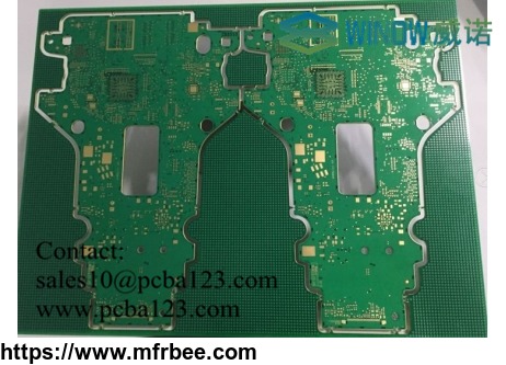
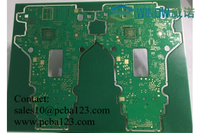
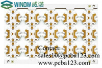
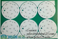
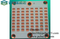
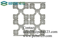
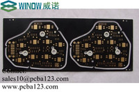
12 Layers High Density Interconnect HDI PCB Circuit Board Fabrication
Product Quick Detail
- Place Of Origin
- China (Mainland)
- Minimum Order
- 1
- Packaging
- N/A
- Delivery
- N/A
Specifications
HDI boards, one of the fastest growing technologies in PCBs, are now available at Eolane SCM. HDI interconnect board contains blind and/or buried vias and often contains microvias of .006 or less in diameter. They have a higher circuitry density than traditional circuit boards.
There are 6 different types of HDI high density interconnect pcb boards, through vias from surface to surface, with buried vias and through vias, two or more HDI layer with through vias, passive substrate with no electrical connection, coreless construction using layer pairs and alternate constructions of coreless constructions using layer pairs.
HDI any-layer printed circuit boards are the next technological enhancement of HDI microvia printed circuit boards: all the electrical connections between the individual layers consist of laser-drilled microvias. The main advantage of this technology is that all the layers can be freely interconnected. To produce these circuit boards, RayMing uses laser-drilled microvias electroplated with copper.
Special technologies used with HDI any-layer printed circuit boards:
•Edge plating for shielding and ground connection
•Minimum track width and spacing in mass production around 40μm
•Stacked microvias (plated copper or filled with conductive paste)
•Cavities, countersunk holes or depth milling
•Solder resist in black, blue, green, etc.
•Low-halogen material in standard and high Tg range
•Low-DK Material for Mobile Devices
•All recognised printed circuit board industry surfaces available
HDI PCBs capitalize on the latest technologies available to increase the functionality of PCBs using the same or less amount of area. This advancement in PCB technology is driven by the miniaturization of components and semiconductor packages that supports advanced features in revolutionary new products. This includes touch screen computing, 4G network communications and military applications such as avionics and smart munitions.
HDI PCBs capitalize on the latest technologies available to increase the functionality of PCBs using the same or less amount of area. This advancement in PCB technology is driven by the miniaturization of components and semiconductor packages that supports advanced features in revolutionary new products. This includes touch screen computing, 4G network communications and military applications such as avionics and smart munitions.
HDI PCBs are characterized by high-density attributes including laser microvias, fine lines and high performance thin materials. This increased density enables more functions per unit area. Higher technology HDI PCBs have multiple layers of copper filled stacked microvias (Advanced HDI PCBs) which creates a structure that enables even more complex interconnections. These very complex structures provide the necessary routing solutions for today’s large pin-count chips utilized in mobile devices and other high technology products.
- Country: China (Mainland)
- Business Type:
- Market:Americas,Europe,Asia,European Union
- Founded Year:1999
- Address:
- Contact:Lucina Lu
You may also like