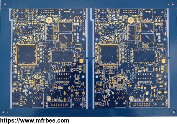
6 layer impedance control PCB
Product sourcing details
- Minimum Order
- 1
- Place Of Origin
- 中国
- Packaging
- 25pcs/bag
- Delivery
- 7days
Specifications
Material: FR4 TG170
Thickness: 1.6mm
Copper thickness: inner layer 1OZ, outer layer 1/1OZ
Min hole size: 0.2mm
Mintrace/spacing: 4/4mil
Solder mask: Blue
Legend: White
Surface finish: ENIG 2u\"
Other: Impedance control.
- Country: China (Mainland)
- Business Type: PCB prototypes manufacturing
- Market: Americas,Europe
- Founded Year: 2007
- Contact: peter lii