PCB Manufacture of 6-layers


Product sourcing details
- Packaging
- box
- Delivery
- <7 Days
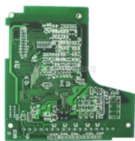
Specifications
specification:
layers : 6;
board thickness : 0.062 inch;
min hole size : 0.011 inch;
solder mask color: red;
silkscreen color : white;
surface : HAL+ hard gold;
others : with gold
- Country: China (Mainland)
- Business Type: Manufacturer
- Market: Africa
- Founded Year: 1997
- Address: Aobei Industrial Zone,Henggang,Shenzhen
- Contact: xiu du