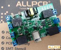
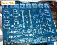
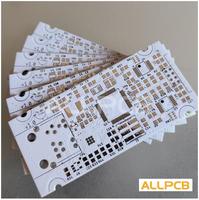
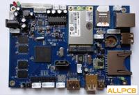
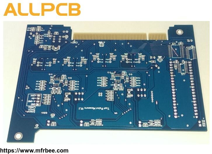
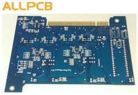
4 layer PCB professional PCB manufacturer in China
Product Quick Detail
- Minimum Order
- 1
- Place Of Origin
- China
- FOB Price
- USD $5.80 / Piece
- Packaging
- VACUUM
- Delivery
- 15 Days
Specifications
4 layer PCB professional PCB manufacturer in China
Description :
Quick Details
Place of Origin:
Anhui,China (Mainland)
Brand Name:
ALLPCB
Model Number:
PCBA-0031
Base Material:
FR4
Copper Thickness:
35um
Board Thickness:
1.6mm
Min. Hole Size:
0.2mm
Min. Line Width:
0.1mm
Min. Line Spacing:
0.1mm
Surface Finishing:
lead free hasl
Solder mask:
Geen
Silkscreen:
white
Board Thickness Tolerance:
±10%
Service:
PCB&PCBA
Certificate:
ISO,UL and ROHS
E-test:
100%
Plugging Vias Capability:
0.2-0.8mm
Inner package:
Vacuum packing
- Country: China (Mainland)
- Business Type: www.allpcb.com/g4 -Full service for PCBs, SMT Stencil and PCBA Free shipping costs for 1st kg Free expedited for 24H/48H
- Market: Americas
- Founded Year: 2003
- Contact: Erin KOU