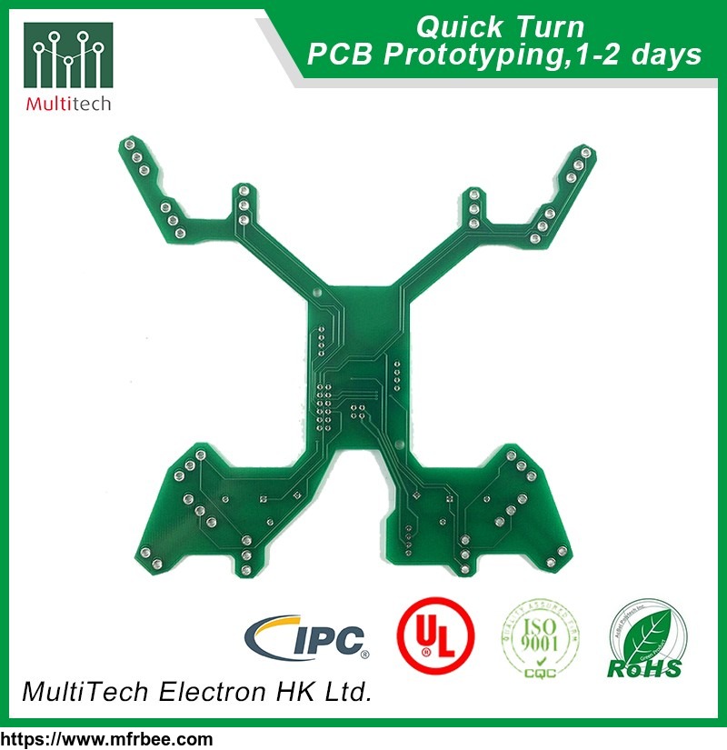
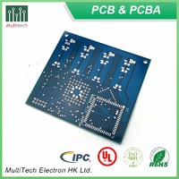
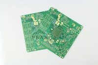
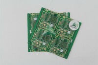
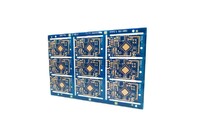
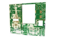
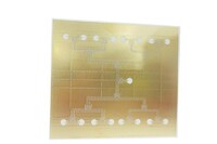
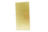
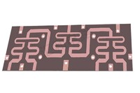
2 layer PCB prototype manufacture
Product Quick Detail
- Minimum Order
- 1
- Place Of Origin
- China
- Packaging
- N/A
- Delivery
- 2~3 Days
Specifications
- Country: China (Mainland)
- Business Type:
- Market:Americas,Europe,Asia,Middle East,European Union,Africa
- Founded Year:2006
- Address:HuangTian No.2 Zhongwu Housing,Baoan District, Shenzhen,China
- Contact:Jon Chen

Other products from Multitech Electron HK Ltd.
Relate products of 2 layer PCB prototype manufacture
HDI PCB Blind/Buried Via 5+N(N+M)+5 Structure Trace Width/Spacing 1.6/1.6mil Laser Hole Size(mm)≥0.075 High Density Interconnector Founded in 2007,PEAK ...
Regular PCB Up to 64 Layers FR4 TG135/TG150/TG170 Halogen Free/CTI≥600 Aspect Ratio (Finish Hole) 28:1 Sample Expedited 8 Hours(1-2Layer) Founded in 2007,PEAK ...
Number of layers: 2 Surface finish: OSP Base material: FR4 Outer Layer W/S: 6/4mil Thickness: 1.0mm Min. hole diameter: 0.25mm Special process: impedance control+half hole Advantages Of 2 Layer OSP Impedance Control Half Hole PCB Own lamination process to convenient production ...
Number of layers: 2 Surface finish: ENIG Base material: FR4 Outer Layer W/S: 7/4mil Thickness: 1.0mm Min. hole diameter: 0.3mm Special process: impedance control+half hole Advantages Of 2 Layer ENIG Impedance Control Half Hole PCB Product Own lamination process to convenient ...
Number of layers: 2 Surface finish: ENIG Base material: FR4 Outer Layer W/S: 8.5/3.5mil Thickness: 0.8mm Min. hole diameter: 0.2mm Special process: half hole Advantages Of Two Sided PCB Own lamination process to convenient production for Multilayer PCB and shorten the lead ...
Number of layers: 2 Surface finish: ENIG Base material: Taconic TLY-5A Min. hole diameter: 0.3mm Outer Layer W: 1.046mil Outer layer S: /mil Thickness: 0.94mm Advantages Of 2 Layer Taconic PCB Own lamination process to convenient production for Multilayer pcb product and ...
Number of layers: 2 size: 184.2*158.9mm Surface finish: LF-HASL Base material: Rogers 4350B Min. hole diameter: 0.4mm Minimum Line Width: 0.227mm Minimum Line Space: 0.127mm Thickness: 0.7mm Advantages Of 2 Layer Rogers LF-HASL PCB Own lamination process to convenient ...
Number of layers: 2 size: 96.45*87.73mm Surface finish: ENIG Base material: Rogers 4350B Min. hole diameter: 0.5mm Minimum Line Width:/mm Minimum Line Space:0.139mm Thickness: 0.35mm Advantages Of 2 Layer Rogers ENIG RF Circuit Board Own lamination process to convenient ...
Number of layers: 2 size: 98.45*49.45mm Surface finish: ENIG Base material: Rogers 4350B Min. hole diameter: 0.5mm Minimum Line Width:/mm Minimum Line Space:0.139mm Thickness: 0.35mm Advantages Of 2 Layer Rogers PCB Own lamination process to convenient production for ...
Number of layers: 2 Surface finish: ENIG Base material: F4B Min. hole diameter: 0.8mm Outer Layer W: 6mil Outer layer S: 6mil Thickness: 1.0mm Advantages Of 2 Layer F4B PCB Own lamination process to convenient production for Multilayer PCB and shorten the lead time. Jiangxi ...