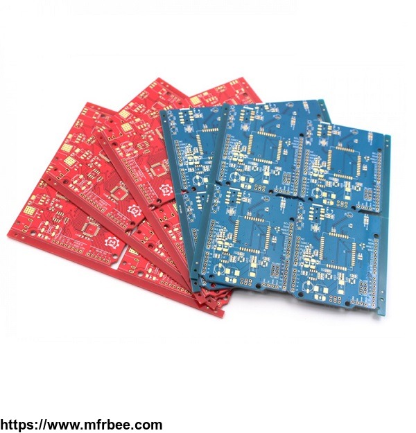
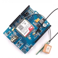
High Quality Low Cost Fast Delivery Printed Circuit Board PCB Provider Makerfabs
Product Quick Detail
- Minimum Order
- 1
- Place Of Origin
- China(Mainland)
- Packaging
- 25pcs each PVC bag
- Delivery
- 4-7 Days
Specifications
The way for the makers & startups to get the PCBs for prototyping or trial-production, with low price while the production and quality control follows all industrial standards.
Gerber Files:
- pcbname.GTL: Top layer
- pcbname.GBL: Bottom layer
- pcbname.GTS: Solder Stop Mask top
- pcbname.GBS: Solder Stop Mask Bottom
- pcbname.GTO: Silk Top
- pcbname.GBO: Silk Bottom
- pcbname.TXT: NC Drill
- pcbname.GML: Mechanical layer
Note:
1. Note that Gerber files must be RS-274x format
2. Drill file(pcbname.TXT) should be Excellon format, and make sure it include drills size and position data
3. Besides the production Gerber files, We also accept PCB files generated by Eagle, Altium Designer, PADS
4. Please leave a comment in the order for special requirements
Spec:
- Layers 1/2/4
- PCB Material FR-4
- Thickness Tolerance (t≥1.0mm) ± 10%
- Thickness Tolerance (t<1.0mm) ± 0.1mm
- Insulation Layer Thickness 0.075mm--5.00mm
- Minimum PCB track 6mil
- Minimum Track/Vias Space 6mil
- Minimum pads Space 8mil
- Minimum silkscreen text size 32mil
- Inner Layer Copper for 4-layer PCB 17um
- Drilling Hole (Mechanical) 0.3mm—6.35mm
- Finish Hole (Mechanical) 0.8mm—6.35mm
- Drill Diameter Tolerance (unplated) 0.05mm
- Drill Diameter Tolerance (plated) 0.1mm
- Outline Tolerance (Mechanical) ±0.20mm
- Aspect Ratio 8:1
- Solder Mask Type Photosensitive ink
- SMT min Solder Mask Width 0.2mm
- Min Solder Mask Clearance 0.2mm
- Solder Mask Thickness 15um
- Country: China (Mainland)
- Business Type: Manufacturer,Trading Company,Distributor/Wholesaler
- Market: Americas,Europe,Asia,Middle East
- Founded Year: 2015
- Address: 401, Huashenghui Office Building, Jinhai Rd, Xixiang Street, Bao'an District
- Contact: Helen He
