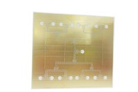
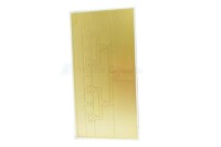
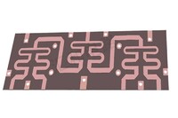
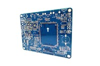
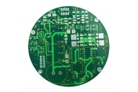
Number of layers 2 size 96.45*87.73mm Surface finish ENIG Base material Rogers 4350B Min. hole diameter 0.5mm Minimum Line Width:/mm Minimum Line Space:0.139mm Thickness 0.35mm Advantages Of 2 Layer Rogers ENIG RF Circuit Board Own lamination process to convenient production
Xinfeng Huihe Circuits Co., Ltd. [2023-04-10 11:02:02 ]
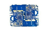
Number of layers 2 size 98.45*49.45mm Surface finish ENIG Base material Rogers 4350B Min. hole diameter 0.5mm Minimum Line Width:/mm Minimum Line Space:0.139mm Thickness 0.35mm Advantages Of 2 Layer Rogers PCB Own lamination process to convenient production for Multilayer PCB
Xinfeng Huihe Circuits Co., Ltd. [2023-04-10 11:01:45 ]
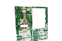
Number of layers 2 Surface finish ENIG Base material F4B Min. hole diameter 0.8mm Outer Layer W 6mil Outer layer S 6mil Thickness 1.0mm Advantages Of 2 Layer F4B PCB Own lamination process to convenient production for Multilayer PCB and shorten the lead time. Jiangxi facility is
Xinfeng Huihe Circuits Co., Ltd. [2023-04-10 11:01:23 ]
DTF printing(Direct to film)is a new technology for garment heat digital screen transfer printing, only need one Inkjet printer, DTF printing ink, and heat-press, saving your cost even for a small quantity run. You can finish the printing CMYK, white inks then shaking adhesive po
JIANGYIN QIANTAI NEW MATERIAL TECHNOLOGY CO.,LTD. [2023-03-16 09:33:53 ]
Number of layers 6 Surface finish HASL Base material FR4 Outer Layer W/S 9/4mil Inner layer W/S 11/7mil Thickness 1.6mm Min. hole diameter 0.3mm Special process Blind Vias Advantages Of 6 Layer HASL Blind Buried Via PCB Own lamination process to convenient production for Multilay
Xinfeng Huihe Circuits Co., Ltd. [2023-02-08 10:06:43 ]
Number of layers 14 Surface finish ENIG Base material FR4 Outer Layer W/S 4/5mil Inner layer W/S 4/3.5mil Thickness 1.6mm Min. hole diameter 0.2mm Special process Blind & Buried Vias Advantages Of 14 Layer PCB Own lamination process to convenient production for Multilayer PCB and
Xinfeng Huihe Circuits Co., Ltd. [2023-02-08 10:06:26 ]
Number of layers 12 Surface finish ENIG Base material FR4 Outer Layer W/S 7/4mil Inner layer W/S 5/4mil Thickness 1.5mm Min. hole diameter 0.25mm Special process Blind Vias Advantages Of 12 Layer PCB Own lamination process to convenient production for Multilayer PCB and shorten t
Xinfeng Huihe Circuits Co., Ltd. [2023-02-08 10:06:11 ]
Number of layers 10 Surface finish ENIG Base material FR4 W/S 4/4mil Thickness 1.6mm Min. hole diameter 0.2mm Special process Blind Vias Advantages Of 10 Layer ENIG Blind Vias PCB Own lamination process to convenient production for Multilayer PCB and shorten the lead time. Jiangx
Xinfeng Huihe Circuits Co., Ltd. [2023-02-08 10:05:55 ]
Number of layers 4 Surface finish ENIG Base material High TG FR4 Outer Layer W/S 4/3.5mil Inner layer W/S 4/3.5mil Thickness 1.0mm Min. hole diameter 0.25mm Special process Impedance Control Advantages Of 4 Layer High TG Impedance Control Fine Pitch PCB Own lamination process to
Xinfeng Huihe Circuits Co., Ltd. [2022-10-20 09:31:30 ]
Number of layers rogers fr4 size:80*88mm Surface finish ENIG Base material FR4+Rogers 4350B Min. hole diameter 0.3mm Minimum Line Width:0.230mm Minimum Line Space:0.170mm Thickness 1.0mm Advantages Of 4 Layer rogers fr4 pcb Own lamination process to convenient production fo
Xinfeng Huihe Circuits Co., Ltd. [2022-10-20 09:30:40 ]
Number of layers 2 Surface finish ENIG Base material Taconic TLY-5A Min. hole diameter 0.3mm Outer Layer W 1.046mil Outer layer S /mil Thickness 0.94mm Advantages Of 2 Layer Taconic PCB Own lamination process to convenient production for Multilayer PCB and shorten the lead time.
Xinfeng Huihe Circuits Co., Ltd. [2022-10-20 09:30:13 ]
Number of layers 2 size 184.2*158.9mm Surface finish LF-HASL Base material Rogers 4350B Min. hole diameter 0.4mm Minimum Line Width 0.227mm Minimum Line Space 0.127mm Thickness 0.7mm Advantages Of 2 Layer Rogers LF-HASL PCB Own lamination process to convenient production for Mult
Xinfeng Huihe Circuits Co., Ltd. [2022-10-20 09:29:48 ]
Number of layers 2 size 96.45*87.73mm Surface finish ENIG Base material Rogers 4350B Min. hole diameter 0.5mm Minimum Line Width:/mm Minimum Line Space:0.139mm Thickness 0.35mm Advantages Of 2 Layer Rogers ENIG Rf PCB Own lamination process to convenient production for Multil
Xinfeng Huihe Circuits Co., Ltd. [2022-10-20 09:29:20 ]
Number of layers 2 size 98.45*49.45mm Surface finish ENIG Base material Rogers 4350B Min. hole diameter 0.5mm Minimum Line Width:/mm Minimum Line Space:0.139mm Thickness 0.35mm Advantages Of 2 Layer Rogers PCB Own lamination process to convenient production for Multilayer PCB
Xinfeng Huihe Circuits Co., Ltd. [2022-10-20 09:28:55 ]
Number of layers 2 Surface finish ENIG Base material F4B Min. hole diameter 0.8mm Outer Layer W 6mil Outer layer S 6mil Thickness 1.0mm Advantages Of 2 Layer F4B PCB Own lamination process to convenient production for Multilayer PCB and shorten the lead time. Jiangxi facility is
Xinfeng Huihe Circuits Co., Ltd. [2022-10-20 09:28:26 ]
Number of layers 16 Surface finish ENIG Base material FR4 Thickness 3.0mm Min. hole diameter 0.35mm size:420×560mm Outer Layer W/S 4/3mil Inner layer W/S 5/4mil Aspect Ratio 9 1 Special process via-in-pad Impedance Control Press Fit Hole Advantages Of 16 Layer ENIG Press Fit H
Xinfeng Huihe Circuits Co., Ltd. [2022-09-16 09:58:30 ]
Number of layers 10 Surface finish ENIG Aspect Ratio 8 1 Base material FR4 Outer Layer W/S 4/4mil Inner layer W/S 5/3.5mil Thickness 2.0mm Min. hole diameter 0.25mm Special process Impedance Control, Resin Plugging, Different Copper Thickness Advantages Of 10 Layer Impedance Cont
Xinfeng Huihe Circuits Co., Ltd. [2022-09-16 09:57:55 ]
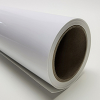
JinYu CF/SPH180D is a double PE coated photo paper for all advertising and photographic prints for indoor applications. High glossy and matte surface are available. It works for solvent ink printers, and this paper also delivers outstanding results with Latex and UV ink systems.
Shanghai JinYu New Materials Co., Ltd. [2022-07-15 16:36:06 ]
Number of layers 8 Surface finish ENIG Base material FR4 Outer Layer W/S 4/3.5mil Inner layer W/S 4/3.5mil Thickness 1.2mm Min. hole diameter 0.2mm Special process impedance control+half hole Advantages Of 8 Layer ENIG Impedance Control Half Hole PCB Own lamination process to con
Xinfeng Huihe Circuits Co., Ltd. [2022-04-27 11:12:41 ]
Number of layers 6 Surface finish LF-HASL Base material FR4 Outer Layer W/S 11/6mil Inner layer W/S 16/5mil Thickness 1.6mm Min. hole diameter 0.3mm Advantages Of 6 layer pcb Own lamination process to convenient production for Multilayer PCB and shorten the lead time. Jiangxi fac
Xinfeng Huihe Circuits Co., Ltd. [2022-04-27 11:11:49 ]
