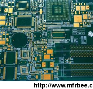
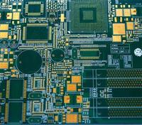
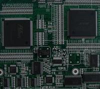
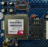
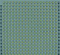
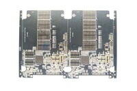
4 Layers PCB
Product Quick Detail
- Packaging
- 12
- Delivery
- 15 Days
Specifications
- Country: China (Mainland)
- Business Type:
- Market:
- Founded Year:1995
- Address:Zhonghuacheng Building, Weiming South Street, Qiaoxi District
- Contact:Jian Zhu
Other products from Polaris Technology Co.,Ltd
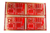
Relate products of 4 Layers PCB

What is FR4? FR4 is the name of a type of epoxy glazing material. fr stands for flame retardant. 4 refers to the factors that differentiate it from other materials. FR4 means two things. The material. As a construction material, it refers to epoxy laminates reinforced with ...
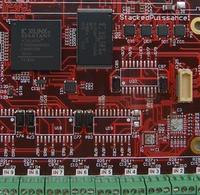
Multilayer PCB Up to 64 Layers; FR4 TG135/TG150/TG170; Halogen Free/CTI≥600; Aspect Ratio (Finish Hole) 28:1; Sample Expedited 8 Hours(1-2Layer); HDI PCB Blind/Buried/Hybrid Via; 5+N(N+M)+5 Structure; Trace Width/Spacing 1.6/1.6mil; Laser Hole Size(mm)≥0.075; High Density ...
The TL-4 burning furnace consists of 3 layers of cylinders. It uses fully burned natural gas to obtain high-temperature flame, and mixing this temperature with fresh air to achieve the required hot air device. Due to the use of fully automatic single-stage fire, two-stage fire ...
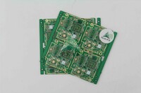
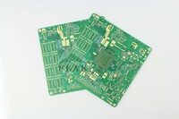
Number of layers: 8 Surface finish: ENIG Base material: FR4 Outer Layer W/S: 4/3mil Inner layer W/S: 4/3mil Thickness: 1.2mm Min. hole diameter: 0.2mm Special process: impedance control Advantages Of 8 Layer PCB Own lamination process to convenient production for Multilayer PCB ...
HDI PCB Blind/Buried Via 5+N(N+M)+5 Structure Trace Width/Spacing 1.6/1.6mil Laser Hole Size(mm)≥0.075 High Density Interconnector Founded in 2007,PEAK ...
What is FR4? FR4 is the name of a type of epoxy glazing material. fr stands for flame retardant. 4 refers to the factors that differentiate it from other materials. FR4 means two things. The material. As a construction material, it refers to epoxy laminates reinforced with ...

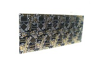
Previous image Next image Number of layers: 16 Surface finish: ENIG Base material: FR4 Thickness: 3.0mm Min. hole diameter:0.35mm size:420×560mm Outer Layer W/S: 4/3mil Inner layer W/S: 5/4mil Aspect Ratio: 9:1 Special process: via-in-pad Impedance Control Press Fit Hole ...

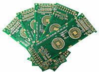
Previous image Next image Number of layers: 10 Surface finish: ENIG Aspect Ratio: 8:1 Base material: FR4 Outer Layer W/S: 4/4mil Inner layer W/S: 5/3.5mil Thickness: 2.0mm Min. hole diameter:0.25mm Special process: Impedance Control, Resin Plugging, Different Copper Thickness ...
Via In pcb board material fr4, using copper plating or epoxy to fill holesfor circuit board factor, prevent solder paste or flux from flowing into the via in pad, avoid solder ball getting into via or solder mask cover on pad and cause false soldering. HUIHE CIRCUITS Via In Pad ...
Number of layers: 8 Surface finish: ENIG Base material: FR4 Outer Layer W/S: 4/3mil Inner layer W/S: 5/4mil Thickness: 1.6mm Min. hole diameter: 0.2mm Special process: half hole Advantages Of 8 Layer ENIG Half Hole Custom Made PCB Own lamination process to convenient production ...